Photoconductive Detectors based on the Photoconductive Effect.
Infrared radiation generates charge carriers in the semiconductor active region decreasing its resistance. The resistance change is sensed as a voltage change by applying a constant current bias. The optimum bias current is specified in the Final Test Report and depends on the detector size, operating temperature, and spectral characteristics.
Photovoltaic Detectors (photodiodes) are semiconductor structures with one (PV) or multiple (PVM) homo- or heterojunctions. Absorbed photons produce electron-hole pairs, resulting in external photocurrent.
Reverse bias voltage may be applied to increase differential resistance, reduce the shot noise, improve high-frequency performance and dynamic range. Reverse bias may increase responsivity in some devices. Unfortunately, at the expense of flicker noise (1/f) in most cases. Photovoltaic detectors are more vulnerable to electrostatic discharges than Photoconductors.
Specifications
- Both, photoconductors & photodiodes available
- Wide range of operating wavelength
- Wide range of chip size (optical area)
- Possibility of temperature sensor assembly (Si diode, thermistor)
- Frequency range up to 1 GHz
- Ready to assembly on thermoelectric cooler
On going
- Parameters and/or geometry can be modified on demand
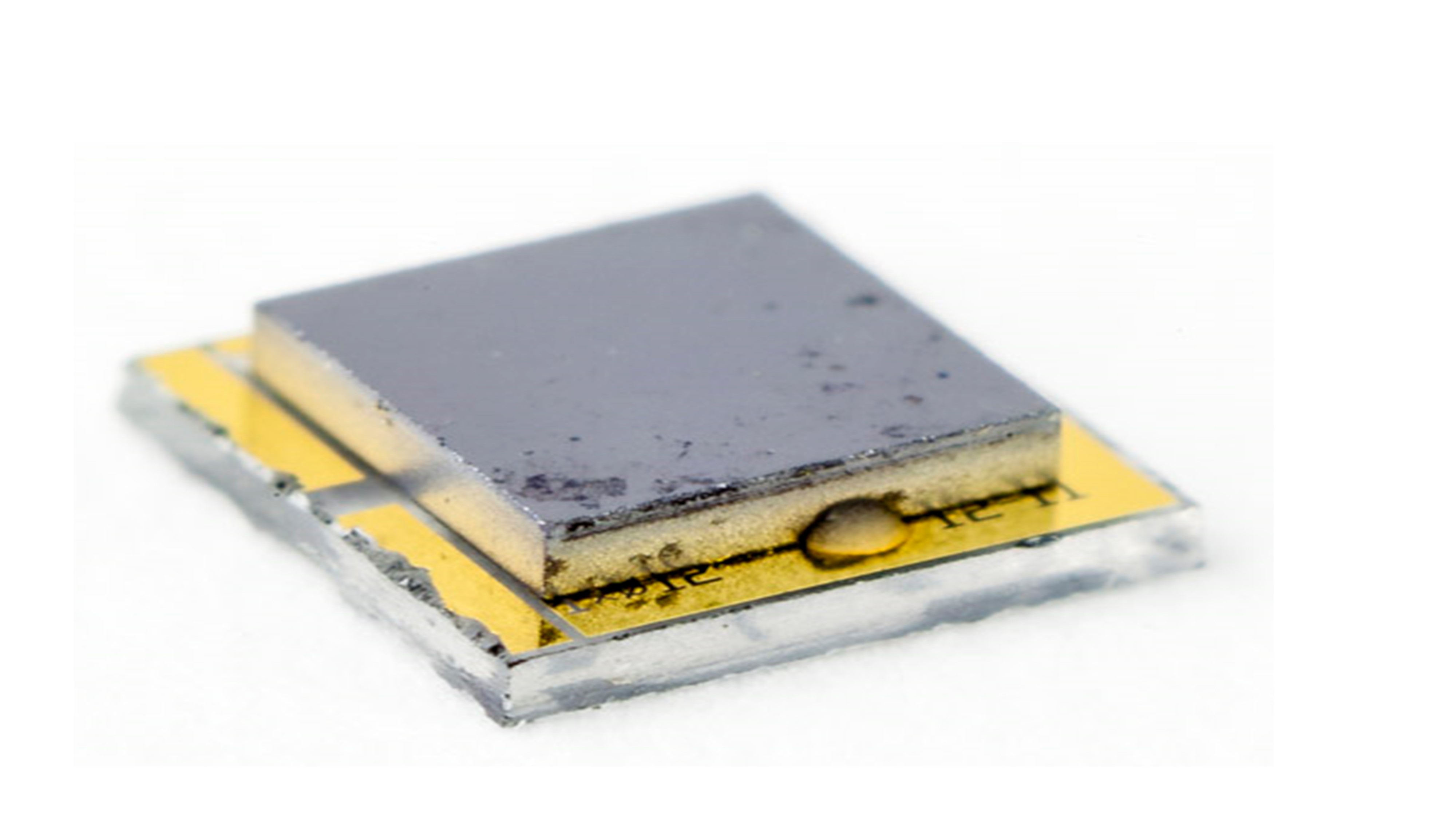
Single detection chip on a sapphire carrier with gold contact pads
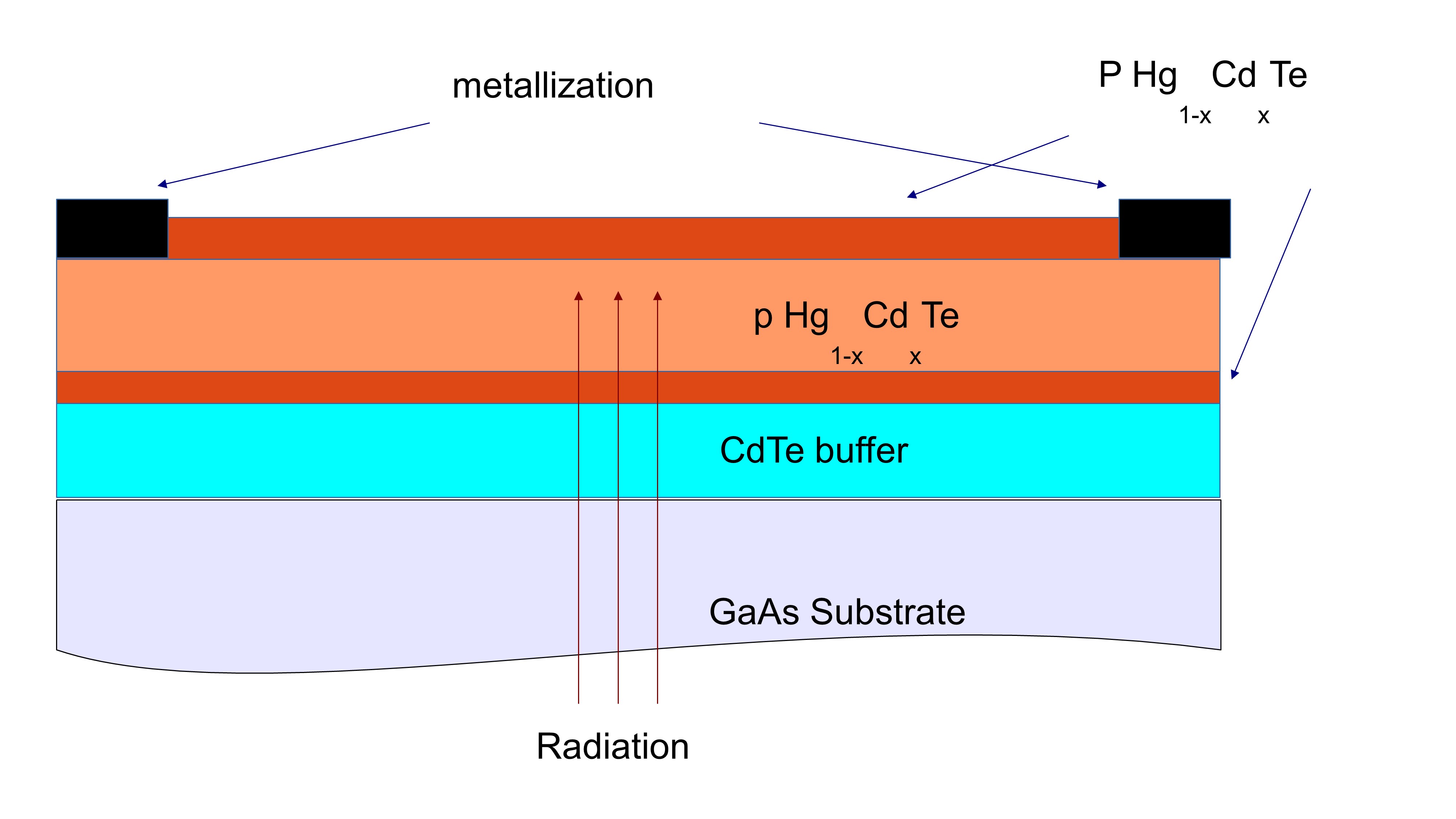
Schematic cross section through layers of a simple photoconductive device without immersion (not in scale)